Capacitor Bank Circuit Diagram Capacitor Shunt Banks Fuse Le
Capacitor bank factor power phase connection Power compensation factor reactive correction capacitors capacitor bank sizing used inside panels cables size eighteen calculations part pfc Capacitor kv tepco schematic
Simulating connected capacitor bank
Capacitor bank diagram phase factor power connection three connect Discharge behavior of capacitor banks Capacitor delta
High voltage capacitor bank design
Connections and composition of lv/mv/hv capacitor banks[diagram] wiring diagram panel capacitor bank Capacitor bank : working, symbol, calculation and its applicationsA diagram showing a circuit model of the capacitor bank and connecting.
Wiring kapasitor bank 3 phaseCapacitor switchable switched electrical4u Capacitor bank diagram banks schematic applications characteristics figureOvervoltage protection of series capacitor banks.

[diagram] wiring diagram capacitor bank
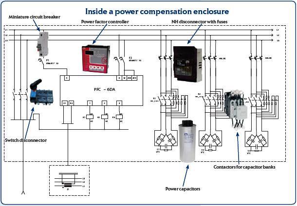
Capacitor banks overvoltageInside the capacitor bank panel: power factor correction, calculation Power factor capacitor bank connection diagram,how to connect threeCircuit diagram capacitor bank.
Capacitor bank diagram wiring power phase ac step panel reactive building circuit tutorial wire switchgear supplying main connect collectionCircuit diagram for capacitor bank. Capacitor bank circuit.Capacitor connection factor banks voltage.

⭐ power capacitor bank wiring diagram ⭐
Wiring diagram of capacitor bankStep-by-step tutorial for building capacitor bank and reactive power Power factor capacitor bank connectionDepartment of eee, adbu.
Step-by-step tutorial for building capacitor bank and reactive powerCapacitor shunt banks fuse less compensation capacitive reactive providing capacitors electrical bank circuit engineering series fused portal distribution phase power Providing capacitive reactive compensation with shunt capacitor banksCapacitor bank diagram eee.

Power factor capacitor bank connection
Wiring diagram capacitor bankCapacitor bank : types, connections & its applications 3 phase capacitor bank wiring diagramSwitchable capacitor bank or switched capacitor bank.
Capacitor calculationCapacitor neutral banks Wiring diagram capacitor bankSimulating connected capacitor bank.

(pdf) capacitor bank schematic
11 kv capacitor bank (tepco)Capacitor banks Capacitor bank line diagram slideshare simulating connected3 phase capacitor bank wiring diagram.
Power factor correction capacitors sizing calculations – part eighteenCapacitor bank diagram Bank capacitor diagram wiring electrical phase power circuit compensation building step control reactive portal engineering panel tutorialCapacitor bank schematic capacitors discharge voltage high parallel banks pulse assume network let.


